Semiconductor Integration : Memory, Logic, Sensor
Semiconductor Integration : Memory, Logic, Sensor
Since 1980, DRAM is the most widely used memory for information delivery, storage and coding. Currently, DRAM products with feature size of 10 nm are emerging, and their market occupied $ 50 billion in the world. As AI and IoT technologies are coming, we believe the global market will continue to grow.
This course is designed for understanding DRAM devices and products. The details of the outline are: (1) Basic operation principle and device structure (2) Development history of DRAM structure and each technical content (3) Experts’ prospect on the structure and development directions of next-generation DRAM. This course intends to provide basic and advance education on DRAM technology for all the technical engineers involved in DRAM-related industries, graduate students, and research institute researchers.
In particular, we describe the process steps that are integrated into three-dimensional X, Y, and Z axes in real time by using our own 3D Image Animation PKG Tool for DRAM cell structure. This program intends to enhance the understanding of the DRAM manufacturing process for material, device, and circuit engineers through a detailed three-dimensional description. This course is designed to provide basic knowledge to graduate students who are interested in DRAM as well as who would like to work in the semiconductor industries.
- Syllabus
Class 1
We will review the development history of the DRAM cell transistor and the DRAM cell capacitor over technology scaling. The target audience of Class 1 includes new employees or graduate students who would like to learn the basics of DRAM memory.
Class 2
Class 2 will be given to engineers and researchers of devices, equipment, and materials companies. The purpose of Class 2 is to understand the process of DRAM cell integration and to explain step-by-step process of DRAM cell fabrication.
Class 3
Class 3 is a more specialized lecture on the process difficulties due to the shrinking of DRAM and trends in technology development. The purpose of Class 3 is to provide advanced technological issues and prospective for next-generation DRAM technology. Class 3 will be given to senior engineers and researchers in fields of semiconductor devices and materials industries or research institutes.
DRAM은 1980년 이후 정보 전달 매체, 저장 및 코딩용으로 가장 많이 사용되는 메모리이다. 현재 10nm대 초반의 선폭을 갖는 제품이 출시 되고 있으며, 2-18년 세계 마켓이 500억불을 점유 하였다. DRAM은 2020년 초반 10nm 이하의 제품 출시가 예상되며 AI, IoT 시대를 맞이하여 앞으로도 세계 마켓이 지속적으로 성장하리라 판단된다.
본 교육은 DRAM 소자 및 제품 이해를 위한 1) 기초 동작 원리 및 소자 구조, 2) DRAM 구조의 변천과정 및 각각의 기술적 내용과 공정 단계별 설명, 그리고 3) 차세대 DRAM의 구조적 전개 및 개발 방향들에 전문가적 의견 제시 및 공유 등을 통해서 , DRAM에 연관된 대학원생, 연구기관의 연구원, 장치 및 소재 업체의 연구원 관련 산업과 관련된 모든 기술직 엔지니어에게 DRAM 기술에 대한 기초 및 심화 교육을 수행하고자 한다.
특히, DRAM 셀 구조에 대해서 자체 개발된 3차원 Image Animation PKG Tool을 이용하여 실시간으로 3차원 X,Y,Z 축으로 집적화 되어가는 공정 단계의 Image View, 공정 난이도가 상대적으로 높은 공정 단계에 대한 3차원적인 자세한 설명을 통해서 소자, 장치 및 소재 전문 엔지니어 대상으로 DRAM 제작 공정의 이해력을 높이고자 한다.
업체 전문 인력 뿐만이니라, DRAM에 관심이 있거나, 이 분야로 취업 하고자 하는 대학원생 들에게, 기초 지식을 함양하도록 하며, 회사 입사 후 배우는 기초 실무 지식에 대한 사전 교육 프로그램도 구비되어 있다.
- Syllabus
Class 1
DRAM의 기초 동작 원리 및 소자 구조에 대한 교육으로 소자의 shrink에 따른 Cell transistor와 cell capacitor의 구조 변경 history를 review하고 소자기술적인 내용 다룬다. 대학원 석 박사 과정, 회사 입사 후 DRAM 메모리 입문 교육 수준으로 강의한다.
Class 2
DRAM 셀 구조 설명, DRAM Cell 대한 공정 단계별 설명을 통해 집적화 과정을 이해시켜서, 전체 구조에 대한 전문적 지식 함양을 목적으로 하는데, 소자, 장치 및 소재 업체의 엔지니어 및 연구소 연구원을 대상으로 강의한다.
Class 3
DRAM의 미세화에 따른 공정의 어려움 및 기술 개발 방향 추이에 대한 보다 특화된 특강으로 문제점을 공유하고 논하며, 해결 방향에 대한 보다 심도 있는 전문지식을 함양 시키기 위한 교육으로, 소자, 장치 및 소재업체의 전문 엔지니어 및 연구소 전문 연구원을 대상으로 강의 한다.
NAND flash memory is currently the most popular memory device. Since the V-NAND product using 3-dimensional structure was developed by Samsung Electronics in 2012, every flash memory company started to develop vertical integration of NAND flash memory.
This course covers basic understanding of NAND flash memory devices and operation: (1) basic operation principle and device structure, (2) fabrication steps for 2-D and 3-D integration, and (3) prospective of next-generation flash memory. We will provide basic and advanced training on flash memory technology to all technical engineers related to flash memory, graduate students, research institute researchers, device and materials industry-related engineers and researchers.
In the class, the 3D Image Animation PKG Tool is used to visualize the device schematics in the 3D X, Y, and Z axes in real time. We intend to provide the understanding of the V-NAND fabrication process using the well-developed 3D Image Animation PKG Tool.
- Syllabus
Class 1
The purpose of Class 1 is to provide a training on basic operation principle and device structure of flash memory. In Class 1, people learn basic flash memory at the beginning level.
Class 2
The purpose of Class 2 is to understand the integration process through the step-by-step description of the 3-D flash memory fabrication. Furthermore, Class 2 covers 2-D and 3-D integration process to provide expert knowledge on NAND flash memory.
Class 3
In Class 3, we provide more specialized lectures on the difficulty of fabrication process as the dimension of the device is shrinking. Furthermore, Class 3 covers the understanding of development in 3-dimensional V-NAND and more in-depth expert knowledge about next-generation NAND flash memory. Lectures will be given to professional engineers and researchers from research institutes and semiconductor industries.
NAND flash 메모리는 현재 저장용으로 가장 많이 사용되는 메모리로써 2012년 이후 삼성전자에 의해서 3차원 구조의 V-NAND 제품이 발표된 이후 모든 flash 메모리 회사에서 수직 셀의 고단화 및 고 집적화 제품 개발에 매진하고 있다.
본 교육은 NAND flash 메모리 소자 및 제품 이해를 위한 1) 기초 동작 원리 및 소자 구조, 2) 2차원 및 3차원 집적화 과정에 대한 공정 단계별 설명, 그리고 3) 미래 flash 메모리의 구조적 전개 및 개발 방향들에 전문가적 의견 제시 및 공유 등을 통해서, flash 메모리에 연관된 대학원생, 연구기관의 연구원, 장치 및 소재 업체의 연구원 관련 산업과 관련된 모든 기술직 엔지니어에게 flash 메모리 기술에 대한 기초 및 심화 교육을 수행하고자 한다.
특히, 3D flash 메모리로 대변되는 삼성전자의 V-NAND 구조에 대해서 자체 개발된 3차원 Image Animation PKG Tool을 이용하여 실시간으로 3차원 X,Y,Z 축으로 집적화 되어가는 공정 단계의 Image View, 공정 난이도가 상대적으로 높은 공정 단계에 대한 3차원적인 자세한 설명을 통해서 소자, 장치 및 소재 전문 엔지니어 대상으로 V-NAND 제작 공정의 이해력을 높이고자 한다.
업체 전문 인력 뿐만이니라, flash 메모리 소자에 관심이 거나, 이 분야로 취업 하고자 하는 대학원생들에게, 기초 지식을 함양하도록 하며, 회사 입사 후 배우는 기초 실무 지식에 대한 사전 교육 프로그램도 구비 되어 있다.
- Syllabus
Class 1
Flash 메모리의 기초 동작 원리 및 소자 구조에 대한 교육으로 대학원 석 박사 과정, 회사 입사 후 flash 메모리 입문 교육 수준으로 강의한다.
Class 2
3차원 flash 메모리 구조 설명, 2차원 및 3차원 집적화 과정에 대한 공정 단계별 설명을 통해 집적화 과정을 이해시켜서, 전체 구조에 대한 전문적 지식 함양을 목적으로 하는데, 소자, 장치 및 소재 업체의 엔지니어 및 연구소 연구원을 대상으로 강의한다.
Class 3
3차원 V-NAND에서 고단화에 따른 공정의 어려움 및 기술 개발 방향 추이에 대한 보다 특화된 특강으로 문제점을 공유하고 논하며, 해결 방향에 대한 보다 심도 있는 전문지식을 함양 시키기 위한 교육으로, 소자, 장치 및 소재업체의 전문 엔지니어 및 연구소 전문 연구원을 대상으로 강의 한다.
X-point array is a technology using emerging memory to address issues of the volatility in DRAM and the speed problem in flash. In recent years, Intel developed an X-point array memory product that uses a phase change material as a memory.
This course introduces (1) the basic principles and device structure of PRAM and X-point array for the understanding of X-point products, (2) the step-by-step fabrication process of 2-dimensional and 3-dimensional integration. We will provide basic and advanced training on -point technology to all technical engineers related to flash memory, graduate students, research institute researchers, device and materials industry-related engineers and researchers.
In particular, we investigate a two-stage X-point array structure of Intel using the 3D Image Animation PKG Tool. We intend to provide the comprehensive understanding of X-point array manufacturing process for device and material engineer through 3-dimensional detailed explanation of process steps.
- Syllabus
Class 1
Class 1 provides basic memory operation principles and device structure of various emerging memories.
Class 2
Class 2 provides the operation principle of X-point array. This course aims to understand the integration process through the step-by-step fabrication process of the integration and to provide expert knowledge on the emerging memory technologies. Lectures will be given to engineers and researchers of device and material industries.
Class 3
The purpose of Class 3 is to share and discuss issues with more specialized lectures. We provide the advanced level of the emerging memory technologies and their trend. Lectures will be given by professional engineers and researchers.
X-point array기술은 DRAM에서는 비휘발성 문제, flash에서는 속도 문제를 동시에 개선 하고자 하면서 집적도도 개선 시키고자 하는 개발 중인 메모리 군이다. 최근 인텔사 등에 의해서 상변화물질을 메모리로 사용하는 X-point array 구조를 갖는 buffer용 메모리 제품이 사용되고 있다.
본 교육은 X-point 메모리 소자 및 제품 이해를 위한 1) PRAM 메모리의 기초 동작 원리 및 소자 구조, 2) 현재 제품으로 사용되는 X-point array 기술의 2차원 및 3차원 집적화 과정에 대한 공정 단계별 설명, 그리고, 3) X-point 기술의 구조적 전개 및 개발 방향들에 전문가적 의견 제시 및 공유 등을 통해서, PRAM, X-point 메모리에 연관된 대학원생, 연구기관의 연구원, 장치 및 소재 업체의 연구원 관련 산업과 관련된 모든 기술직 엔지니어에게 PRAM, X-point 메모리 기술에 대한 기초 및 심화 교육을 수행하고자 한다.
특히, 인텔사, 마이크론사의 2단 X-point array 구조에 대해서 자체 개발된 3차원 Image Animation PKG Tool을 이용하여 실시간으로 3차원 X,Y,Z 축으로 집적화 되어가는 공정 단계의 Image View, 공정 난이도가 상대적으로 높은 공정 단계에 대한 3차원적인 자세한 설명을 통해서 소자, 장치 및 소재 전문 엔지니어 대상으로 X-point array 제작 공정의 이해력을 높이고자 한다.
업체 전문 인력 뿐만이니라, flash 메모리 소자에 관심이 거나, 이 분야로 취업 하고자 하는 대학원생들에게, 기초 지식을 함양하도록 하며, 회사 입사 후 배우는 기초 실무 지식에 대한 사전 교육 프로그램도 구비 되어 있다.
- Syllabus
Class 1
PRAM, X-point array 메모리의 기초 동작 원리 및 소자 구조에 대한 교육으로 대학원 석 박사 과정, 회사 입사 후 관련 메모리 입문 교육 수준으로 강의한다.
Class 2
PRAM, X-point array 구조 설명집적화 과정에 대한 공정 단계별 설명을 통해 집적화 과정을 이해시켜서, 전체 구조에 대한 전문적 지식 함양을 목적으로 하는데, 소자, 장치 및 소재 업체의 엔지니어 및 연구소 연구원을 대상으로 강의한다.
Class 3
PRAM, X-point array에서 고단화 및 미세화의 어려움 및 기술 개발 방향 추이에 대한 보다 특화된 특강으로 문제점을 공유하고 논하며, 해결 방향에 대한 보다 심도 있는 전문지식을 함양 시키기 위한 교육으로, 소자, 장치 및 소재업체의 전문 엔지니어 및 연구소 전문 연구원을 대상으로 강의 한다.
STT-MRAM is a technology using emerging memory to address issues of the volatility in DRAM and the speed problem in flash. In recent years, Samsung Co. etc have developed an STT-MRAM as the replacement of SRAM in system LSI.
This course introduces (1) the basic principles and device structure of MRAM and STT-MRAM for the understanding of magnetic memory, (2) the step-by-step fabrication process of 2-dimensional and 3-dimensional integration. We will provide basic and advanced training on -point technology to all technical engineers related to MRAM, graduate students, research institute researchers, device and materials industry-related engineers and researchers.
In particular, we investigate recent product from spintec and everspin, using the 3D Image Animation PKG Tool. We intend to provide the comprehensive understanding of MRAM and STT-MRAM manufacturing process for device and material engineer through 3-dimensional detailed explanation of process steps.
- Syllabus
Class 1
Class 1 provides basic memory operation principles and device structure of MRAM and STT-MRAM.
Class 2
Class 2 provides the operation principle of STT-MRAM. This course aims to understand the integration process through the step-by-step fabrication process of the integration and to provide expert knowledge on STT-MRAM technologies. Lectures will be given to engineers and researchers of device and material industries.
Class 3
The purpose of Class 3 is to share and discuss issues with more specialized lectures. We provide the advanced level of the STT-MRAM memory technologies and their trend. Lectures will be given by professional engineers and researchers.
STT-MRAM 기술은 2010년 중반 DRAM 대체를 위한 핵심 Emerging Memory로 반도체 소자 업체에서 개발되어 왔다. 현재 미세화를 제품 기술이 삼성전자 등에서 개발되었고, System LSI에서 SRAM을 대체 할 수 있는 Embedded Memory로 자리를 잡고 있다. STT-MRAM은 SRAM 수준의 고속 동작과 다른 비휘발성 대비 우수한 신뢰성 특성으로 앞으로 Emerging Memory의 위치를 더욱 확고 해 질 전망이다.
본 교육은 MRAM, STT_MRA 소자 및 제품 이해를 위한 1) 메모리의 기초 동작 원리 및 소자 구조, 2) 현재 제품으로 사용되는 MRAM, STT-MRAM 기술의 2차원 및 3차원 집적화 과정에 대한 공정 단계별 설명, 그리고, 3) STT-MRAM 기술의 구조적 전개 및 개발 방향들에 전문가적 의견 제시 및 공유 등을 통해서, MRAM, STT-MRAM에 연관된 대학원생, 연구기관의 연구원, 장치 및 소재 업체의 연구원 관련 산업과 관련된 모든 기술직 엔지니어에게 MRAM, STT-MRAM 기술에 대한 기초 및 심화 교육을 수행하고자 한다.
특히, spintec, everspin사의 출시된 MRAM, STT-MRAM 자체 개발된 3차원 Image Animation PKG Tool을 이용하여 실시간으로 3차원 X,Y,Z 축으로 집적화 되어가는 공정 단계의 Image View, 공정 난이도가 상대적으로 높은 공정 단계에 대한 3차원적인 자세한 설명을 통해서 소자, 장치 및 소재 전문 엔지니어 대상으로 MRAM, STT-MRAM 제작 공정의 이해력을 높이고자 한다.
업체 전문 인력 뿐만이니라, MRAM, STT-MRAM 소자에 관심이 거나, 이 분야로 취업 하고자 하는 대학원생 들에게, 기초 지식을 함양하도록 하며, 회사 입사 후 배우는 기초 실무 지식에 대한 사전 교육 프로그램도 구비 되어 있다.
- Syllabus
Class 1
MRAM의 기초 동작 원리 및 소자 구조에 대한 교육으로 대학원 석 박사 과정, 회사 입사 후 관련 메모리 입문 교육 수준으로 강의한다.
Class 2
STT-MRAM 구조 설명집적화 과정에 대한 공정 단계별 설명을 통해 집적화 과정을 이해시켜서, 전체 구조에 대한 전문적 지식 함양을 목적으로 하는데, 소자, 장치 및 소재 업체의 엔지니어 및 연구소 연구원을 대상으로 강의한다.
Class 3
STT-MRAM 미세화의 어려움 및 기술 개발 방향 추이에 대한 보다 특화된 특강으로 문제점을 공유하고 논하며, 해결 방향에 대한 보다 심도 있는 전문지식을 함양 시키기 위한 교육으로, 소자, 장치 및 소재업체의 전문 엔지니어 및 연구소 전문 연구원을 대상으로 강의 한다.
In this tutorial, I will cover to understand the logic technology, history and progress, including future challenges. It will contain what the logic product is, logic structure and how they are manufactured, what the key processes and their purpose. It also reviews the common logic competition metric (speed, power, density, cost) and what is main device performance sensitive parameter and what is going on to get technical problems and solutions. More details are difficulties of key unit/module processes, device structure and material change including BEOL interconnect. In particular, it describes the process steps integrated into three dimensions using its own 3D image animation tools for logical standard cell structures. The program is also intended to improve understanding of the logic manufacturing process for material, device, and circuit engineers.
- Syllabus
Class 1
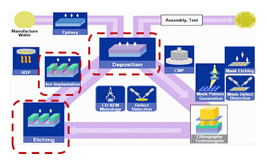
Introduction to Basic Electronics and Microelectronics Terms, Define Process Nodes, Device Physics and transistor operation, Crystal Growth and Wafer Prep. The course covers CMOS fundamental IC manufacturing technologies for logic application. We will also cover the development history of the logic device and conventional technology scaling. The target audience of Class 1 includes new employees or graduate students who would like to learn the basics of logic device and technology. How circuit design impacts to device, manufacturing, mask making, and wafer processing. Additional topics include wafer processing steps such as mask generation, lithography, (including EUV), Deposition (CVD, electro-plating, ALD and sputtering), oxidation, diffusion, implant, RTP, etching and CMP.
Class 2
Class 2 will be given to engineers and researchers of devices, equipment, and materials companies. The purpose of Class 2 is to understand the process integration and to explain step-by-step process of logic fabrication. We will cover the current issues in process integration and breakthrough.
Class 3
Class 3 is a more specialized lecture on the process challenges due to the shrinking and trends in technology development. The purpose of Class 3 is to provide advanced technological issues and solutions for next-generation logic technology. Class 3 will be given to senior engineers and researchers in fields of semiconductor devices and materials industries or research institutes.
Embedded Flash (e-Flash) memory is a key enabling technology for many programmable semiconductor products requiring small form factor and low-power processing. For example, microcontrollers use e-Flash to store program instructions (code) as well as data on which processing is performed. Non-Volatile Memory (NVM) includes the industry common One-Time-Programmable memory (OTP), Multiple-Time-Programmable memory (MTP), Flash memory (Flash), and next generation NVM of Magnetic RAM (MRAM). Embedded Flash support a wide range of applications including consumer electronics, portable electronics, home appliances, smartcards, computers, wired and wireless communications, automotive electronics, medical equipment, industrial automation, the Internet of Things, and wearables.
Current volume production of Embedded Flash technology is 40nm, and is developing the 28nm Embedded Flash. Industry is also developing Embedded MRAM to fulfill customers’ need of continuous performance improvement and power-consumption reduction. Through IP customization, MRAMs can serve various applications, such as artificial intelligence and e-Flash replacement for MCU.
This course is designed to provide basic knowledge to graduate students who are interested in embedded NVM technology as well as who would like to work in the semiconductor industries. After completing this course, the student will have understanding of current logic manufacturing processes including embedded process.
- Syllabus
Class 1
This course covers basic e-Flash cell structure, device operation. and application to basic Electronics and Microelectronics. The course covers CMOS fundamental IC manufacturing technologies for e-Flash application. We will also cover the development history of the e-Flash device and conventional technology scaling. The target audience of Class 1 includes new employees or graduate students who would like to learn the basics of logic device and technology.
Class 2
Class 2 will be given to engineers and researchers of devices, equipment, and materials companies. The purpose of Class 2 is to understand the process integration and to explain step-by-step process of e-Flash fabrication. We will cover the current issues in process integration and breakthrough.
Class 3
Class 3 is a more specialized lecture on the process challenges due to the shrinking and trends in technology development. The purpose of Class 3 is to provide advanced technological issues and solutions for next-generation e-Flash technology including e-MRAM. Class 3 will be given to senior engineers and researchers in fields of semiconductor devices and materials industries or research institutes.
Empty tab. Edit page to add content here.
Semiconductor Process
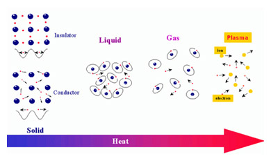
Plasma technology lecture is for basic understanding of plasma fundamental and its application in semiconductor and display fabrication process. Plasma technologies are applied in various fabrication process such as etching, ion implantation and dry cleaning, etc.
This covers from basic and principle for plasma to real application for engineer, researcher in industry and graduate student in university.
material transition
application of plasma technology
- Syllabus
Class 1
Contents for plasma basic are related to electromagnetic characteristics for plasma, plasma structure, and it generation principle. This lecture is for graduate student in university and new engineer in industry.
Class 2
Plasma sources in DC, RF plasma (ICP, CCP) are introduced. Various
applications such as etch, ion implantation and cleaning are discussed.
Finally, plasma monitoring technology is explained, too.
플라즈마 공학은 반도체/디스플레이 제조 공정에 사용되는 공정 플라즈마에 대한 기초 강의로 플라즈마 이해와 플라즈마 응용 분야를 배운다. 플라즈마가 주로 응용되는 분야는 식각, 증착, 이온 주입, 세정 등 여러 공정에 응용되고 있다.
플라즈마를 이해하고자 하는 분과 이를 응용하는 분들을 위해 플라즈마 기초에서 응용까지 다루는 강의를 준비하였다.
물질의 상태
플라즈마 응용 분야
- Syllabus
Class 1 : 플라즈마 기초
물질의 네번째 상태인 플라즈마의 전자기 특성과 플라즈마 구조 및 생성 원리 등을 다룬다.
Class 2 : 플라즈마 소스 및 응용
DC, RF 플라즈마(ICP, CCP) 등 플라즈마 소스를 다룬다. 또한, 플라즈마를 이용한 다양한 반도체 응용 분야에 대해서 강연한다.
DRAM and NAND flash memory devices are being actively developed from two-dimensional to three-dimensional structures for further integration and performance improvement. According to the ITRS, 7nm Logic, 14nm DRAM and 128-stage NAND flash memory devices will be launched in earnest starting in 2020.At this point, realization and commercialization of ASP (Atomic Scale Process) are becoming more important. To realize 3D structures such as 3D-NAND and 3D-FinFET for low power and large capacity, it is necessary to deeply understand ALD technology for atomic level process deposition.
This lecture aims to provide the understanding of the core technology of ALD deposition process which compromise excellent step coverage, thickness uniformity and composition uniformity in nanoscale device structure. In this lecture, contents were organized to develop basic knowledge of ALD to researchers and engineers of semiconductor devices, materials, and equipments’ companies as well as undergraduate / graduate students who are passionate about semiconductor technologies.
- Syllabus
Class 1
In Class 1, ALD process operation mechanism is explained and lecture will be conducted to reach the basic level of graduate student course and explore various functional thin film material (metal, insulator, semiconductor) deposition equipment and their fundamental operation principles.
Class 2
Class 2 provides more specialized lectures on ALD process such as ZrO2 dielectric thin film applied to DRAM capacitor, HfO2 dielectric layer applied to FinFET. The target audience of Class 2 is engineers of device, equipment and material company and research institute researchers.
Class 3
Ultra-thin film deposition by advanced ALD technology can overcome high shrinkage issue and scaling down in three-dimensional V-NAND and DRAM devices as the ALD technology has excellent step coverage. In Class 3, we aims to provide in-depth understanding on future trends in ALD technology development, which targets senior engineers and researchers in device, equipment and material companies.
DRAM 및 NAND flash 메모리 소자는 지속적인 집적도 증대 및 성능향상을 위하여 2차원에서 3차원 구조로 발전하고 있다. ITRS에 따르면 2020년부터 7nm급 Logic, 14nm DRAM, 128단 NAND등의 제품이 본격적으로 출시될 예정으로 이를 위한 10nm 이하 극초미세 원자수준공정 (ASP: Atomic Scale Process) 제조기술 상용화 및 원천기술 확보가 중요해지고 있다.
향후 저전력과 대용량을 위한 3D NAND, FinFET등 3차원 구조를 구현하기 위해서는 원자수준공정 증착이 가능한 ALD 기술에 대한 심층적인 이해가 필수적이다. 본 강의에서는 나노 스케일 트렌치 구조에 우수한 단차 피복성, 두께 균일성, 조성 균일성을 만족시키는 ALD 증착 공정의 핵심요소기술 이해를 증진시키고자 한다.
반도체 분야에 관심이 있거나, 이 분야 진출을 희망하는 학부/대학원생은 물론이고 반도체 소자, 소재, 장비업체 전문연구원 및 엔지니어에게 ALD 기초 지식 및 전문 공정 지식을 함양할 수 있도록 강의내용을 구성하였다.
- Syllabus
Class 1
ALD 공정 기초적 증착 기구를 설명하고, 다양한 기능성 박막재료 (금속, 절연체, 반도체) 증착 장비 및 증착 원리에 대한 교육을 통하여 유관 대학원과정 및 기업체 입문 수준에 도달할 수 있도록 강의를 진행한다.
Class 2
DRAM Capacitor 공정에 적용하는 ALD ZrO2 유전 박막, FinFET 소자에 적용되는 ALD HfO2 유전 박막 요구사항과 이를 달성하기 위한 공정 제어 및 물성 해석에 대한 전문적 지식 함양을 목적으로 하며, 소자, 장비 및 소재 업체의 엔지니어 및 연구소 연구원을 대상으로 강의한다.
Class 3
3차원 V-NAND, DRAM 소자에서 진행되는 지속적인 고단화, 스케일링 다운에 대응 가능한 매우 얇고, 단차피복성이 우수한 ALD 증착 기술 이슈 및 향후 기술 개발 방향 추이에 대한 심도 있는 전문지식을 함양을 목표로 하며, 소자, 장비 및 소재업체의 전문 연구원/엔지니어를 대상으로 강의 한다.
On Preparing…
On Preparing…
Semiconductor Technology for AI
This course covers (1) introduction of synapse device by explaining basic concept of the weight change, (2) understanding of memristor device to mimic synapse, and (3) technology trend of neuromorphic chips using synaptic memory. The purpose of this course is to enhance the understanding of Synapse devices for graduate students studying AI, researchers at research institutes, engineers at device and material-related companies, and engineers working on neural hardware engineering, The goal is to motivate researchers or students to contribute to more AI industry by acquiring better understanding of neuromorphic devices and circuits.
Many kinds of neural hardware applications have been intensively developed. This lecture aims to provide better understanding of synapse devices’ basic introduction including operation principle and technology directions to engineers and researchers. We aim to make them have a clear idea through the accurate comparison of synapse devices based on conventional memristors.
- Syllabus
Class 1
In Class 1, we provide lecture on basic principles of synapse device. Furthermore, characteristics of memristor devices will be explained, which would be helpful to graduate student and engineers/researchers who are passionate about neuromorphic devices.
Class 2
In addition to the lectures on synapse devices using conventional SRAM and DRAM, it is necessary to understand the integration process of memristor devices. Furthermore, Class 3 aims to educate the characteristics of new synapse devices using memristors. Lectures will be given to engineers and researchers at materials and devices-related research institutes.
Class 3
Class 3 provides a more specialized lecture on the development strategy and direction by sharing the characteristics of synapse device as well as possible applications based on synapse networks. Lectures will be given by professional engineers and researchers to provide in-depth discussion of current issues and expert-level knowledge on synapse device and its applications.
본 교육은 Neuromorphic Chip의 Weight를 저장하고 Processing 하는데 가장 기본이 되는 Synapse소자의 1) 동작 원리 및 종류, 2) 최근 Synapse 소자로 각광 받는 Memristor Device에 대한 이해그리고 3) 최신 Synapse 소자에 대한 연구 동향과 미래 개발에 관한 전문가적 의견 제시 및 공유 등을 통해서, Neural Hardware뿐 아니라 AI 산업에 연관된 대학원생, 연구기관의 연구원, 장치 및 소재 업체의 연구원 그리고 AI 산업과 관련된 모든 엔지니어에게 Synapse 소자에 대한 이해를 높이고, 앞으로 미래 주요 산업인 AI Hardware의 중심인 synapse를 통해서 더 높은 지식을 획득함으로서 좀 더 많은 AI 산업에 기여할 기회를 제공하는데 그 목표가 있다.
최근 AI 산업의 폭발적인 관심으로 인해서 수많은 종류의 AI 응용과 이를 위한 새로운 전용 Software, Hardware 기술들이 소개되고 있어서 자칫 일반인은 물론 관련 연구자들도 혼란을 일으킬 수 있다. 이 강의는 역사적 배경 뿐 아니라 기존의 인공지능 Synapse와Memristor 기반의 Synapse에 대한 정확한 비교를 통해서 이에 관심있는 공학도, 개발자, 연구자들이 확실한 개념을 가지게 하고자하고 이를 통해서 미래 Sysnapse 소자에 대한 연구 방향을 확실히 할 수 있을 것을 기대한다.
- Syllabus
Class 1
Synapse 소자의 기초 동작 원리 및 Memristor 소자의 특성에 대한 교육으로 대학원 석 박사 과정, 회사 입사 후 입문 교육 수준으로 강의한다.
Class 2
SRAM, DRAM을 활용한 Synapse 소자의 기본 동작 특성 뿐 아니라, 최근 각광 받는 Memristor 소자의 특성을 뿐 아니라 집적화 과정을 이해시켜서, 전체 구조에 대한 전문적 지식 함향하고 이를 이용한 새로운 Synapase 소자의 특성을 교육하여, 장치 및 소재 업체의 엔지니어 및 연구소 연구원을 대상으로 강의한다.
Class 3
Synapse 소자의 특성 뿐 아니라 관련된 응용과의 연계성을 이해 시킴으로서 개발 전략 및 방향을 이해할 수 있는 보다 특화된 특강으로 문제점을 공유하고 논하며, 심도있는 전문지식을 함양 시키기 위한 교육으로, 소자, 장치 및 소재업체의 전문 엔지니어 및 연구소 전문 연구원을 대상으로 강의 한다.
This course is about neuromorphic chip for parallel neural computing to overcome the problem of conventional Von Neumann computing. This course deals with (1) operation principle and characteristics of neuromorphic chip, (2) relationship between neuromorphic chip and synapse device, and (3) comparison and discussion of processing near memory (PNM) and processing in memory (PIM) by sharing of expert opinions on future prospective. In addition to neural hardware engineers, researchers at research institutes, engineers at semiconductor companies would be able to get better understanding and our target is to provide them opportunities to contribute to more AI industry by increasing their understanding of neuromorphic chips.
Due to the emerging interest of the AI industry, all most researches introduce a variety of neuromorphic chips. This lecture aims to provide better understanding of neuromorphic chip including operation principle and technology directions to engineers and researchers. Through this course, engineers, developers, and researchers would be able to have a clear understanding, and accordingly they would be able to contribute the future technology development on neuromorphic chip.
- Syllabus
Class 1
Class 1 provides lecture on basic principles and types of neuromorphic chip to graduate student, researchers, and engineers with as high as introduction level of flash memory after joining company.
Class 2
In Class 2, lectures will be given to engineers and researchers of semiconductor companies by providing a deep understanding of neuromorphic chip by comparing and analyzing various neuromorphic chips, which are being currently developed in semiconductor industries.
Class 3
Class 3 is a special lecture to learn neuromorphic chip with architecture level. This class aims to share the pros and cons of PNM, PIM (or CIM*) architecture. Lectures will be given by professional engineers and researchers to share expert-level knowledge and technology trend.
CIM* = Computing In Memory
본 교육은 기존의 Von Neumann 방식의 Computing 의 문제를 극복하기 위한Parallel하고 Distributed 방식의 Neural Computing 을 위한 Neuromorphic Chip 에 대한 것이다.
세부 교육 내용은 Neuromorphic Chip의 1) 동작 원리와 특징, 2) Synapse Device와 Neuromorphic Chip의 관계와 동작 원리 그리고 3) PNM(Processing Near Memory)과 PIM(Processing In Memory)에 대한 비교와 장/단점 그리고 미래 전망 에 관한 전문가적 의견 제시 및 공유 등을 통해서 , Neural Hardware뿐 아니라 AI 산업에 연관된 대학원생, 연구기관의 연구원, 장치 및 소재 업체의 연구원 그리고 AI 산업과 관련된 모든 엔지니어에게 Neuromorphic Chip에 대한 이해를 높이고 더 높은 지식을 획득함으로서 좀 더 많은 AI 산업에 기여할 기회를 제공하는데 그 목표가 있다.
최근 AI 산업의 폭발적인 관심으로 각기업과 학겨들이 수많은 종류의 Neuromorphic Chip을 소개하고 있으며 이를의 구조와 동작 특성들을 비교 분석하여 Chip 간의 장단점을 이해하고 이를 바탕으로 가장 바람직한 Neuromorphic Chip 에 대해서 함께 고민하는 시간을 갖고자 한다. 이 교육을 통해서 이에 관심있는 공학도, 개발자, 연구자들이 확실한 개념을 가지게 하고자하고 이를 통해서 미래 Neuromorphic Chip 대한 연구 방향을 확실히 할 수 있을 것을 기대한다.
- Syllabus
Class 1
Neuromorphic Chip의 기초 동작 원리 및 종류에 대한 교육으로 대학원 석 박사 과정, 회사 입사 후 flash 메모리 입문 교육 수준으로 강의한다.
Class 2
현재 연구개발 중인 다양한 Neuromorphic Chip을 비교 분석하고 그 특성에 대해서 이해함으로서 Neuromorphic Chip에 대한 지식을 심화하 과정으로, 소자, 장치 및 소재 업체의 엔지니어, 연구소 연구원을 대상으로 강의한다.
Class 3
Neuromorphic Chip의 Architecture에 대해 심화 학습하는 특강으로 PNM, PIM(또는 CIM*) Architecture의 장단점을 공유하고 논하며, 해결 방향에 대한 보다 심도 있는 전문지식을 함양 시키기 위한 교육으로, 소자, 장치 및 소재업체의 전문 엔지니어 및 연구소 전문 연구원을 대상으로 강의 한다.
CIM* = Computing In Memory
Empty tab. Edit page to add content here.
This lecture will cover the basics and applications of artificial intelligence. Recently, artificial intelligence has made a lot of progress in its performance with the advent of Deep Learning technique. Such machine-learning technology has achieved unprecedented improvements in processing video, speech and natural language, and is expected to be applied in various fields such as automobiles, robots, semiconductors and factories to achieve innovative developments leading to the fourth industrial revolution.
In this lecture, we learn the fundamentals and principles of these machine learning techniques and explain the key theories. First, we introduce the concept and purpose of machine learning and take a look at the basics of deep neural network model. We explore the widely used architectures such as convolutional neural network (CNN) and recurrent neural network (RNN) used to analyze images and time series data. We also introduce the principles of reinforcement learning. Next, we present case-based analysis of how artificial intelligence technology is applied to a variety of engineering areas including semiconductor and hardware design. By taking this course, the students will be able to understand the basic principles of deep learning technology and see how it can make today’s devices and systems more intelligent and advanced. In addition, they will have the opportunity to discuss how to apply artificial intelligence on the problems he is dealing with.
- Syllabus
Class 1
In class 1, we learn the basic theory of machine learning. The students will understand the concept and purpose of machine learning and the basic deep neural network.
Class 2
In class 2, we explain the most commonly used convolutional neural network (CNN) and recurrent neural network (RNN) models and examine the principles and application of these models. We will also take a quick look at the basic principles of reinforcement learning.
Class 3
In class 3, we study various applications of artificial intelligence. We analyze various cases of application of deep learning including image recognition, super resolution, object detection and semantic segmentation. The students will have chance to discuss how to apply artificial intelligence to their own problems.
본 강의에서는 인공지능의 기초와 응용에 대해 다루고자 한다. 최근 인공지능은 딥러닝이라는 머신러닝 모델이 출현함에 따라 그 성능에 많은 발전을 이루었다. 이러한 머신러닝 기술은 영상, 음성, 자연어들을 처리하는 데 전례없는 성능의 개선을 이루었고 자동차, 로봇, 반도체, 공장 등의 다양한 분야에 적용되어 4차산업혁명을 이끄는 혁신적인 발전을 가져올 수 있을 것으로 예상되고 있다.
본 강의에서는 이러한 머신러닝 기술의 기초과 원리를 파악하고 핵심 이론에 대해서 설명한다. 머신러닝의 개념과 목적을 파악하고 딥신경망 모델과 기본적인 트레이닝 기법에 대해 살펴본다. 영상과 시계열 데이터를 학습하기 위한 Convolutional neural network (CNN)과 Recurrent neural network (RNN) 구조를 살펴보고 강화학습의 원리에 대해서도 살펴본다. 이러한 지식을 기반으로 반도체 및 하드웨어 설계 및 공정을 포함한 다양한 공학 분야에 인공지능 기술이 어떻게 적용되는 지에 대해 사례를 중심으로 분석하고자 한다.
본 강의를 수강함으로써 학생들이 요즘 많은 관심을 받고 있는 딥러닝 기술의 기본적인 원리를 파악하게 되고 이러한 기술이 현재의 디바이스 및 시스템을 어떻게 지능화시키고 발전시킬 수 있는 지를 이해할 수 있게 될 것이다. 아울러 본인이 다루고 있는 분야에 대해 인공지능의 적용 방안을 스스로 제안해 볼 수 있는 기회를 갖게 될 것이다.
- Syllabus
Class 1
Class 1 에서는 머신러닝의 기초 이론에 대해서 배운다. 머신러닝의 개념과 목적 그리고 기본적인 딥뉴럴네트워크에 대한 이해를 목적으로 한다.
Class 2
Class 2 에서는 가장 많이 사용되는 딥뉴럴네트워크 구조인 Convolutional neural network (CNN)과 Recurrent neural network (RNN) 모델을 살펴보고 원리와 적용방법을 살펴본다. 강화학습의 기본 원리에 대해서도 간단히 살펴본다.
Class 3
Class 3 에서는 인공지능 기술의 적용 사례를 분석한다. 영상 분석, 물체 검출, 영역 분할등의 다양한 인공지능 응용 사례를 분석하고 학생들이 각자 자신의 분야에서 어떻게 인공지능을 적용할 수 있을지에 대해 토의한다.